Category: Projects
2012
06.26

Recently I’ve been thinking about how I’d really like to make more progress on my projects and how I feel some amount of accountability would help with that. To that end, I’ve decided to start posting regular updates of my projects! Normally I like to save them up and reveal them once completed, but I think seeing feedback from readers will help to motivate me to continue moving forward on projects that might otherwise sit on the workbench for weeks, plus some people might be interested in the details of my design process (at least I might some day in the future, looking back at these posts).

To start things off, I’ll write my first progress report on my bluetooth Kinesis mod. Earlier this year I wrote about my new-to-me keyboard, the Kinesis Essential. I have a few friends who also have this style of keyboard and one of them asked me if I could convert it to bluetooth for him. We did some brainstorming, ordered some parts, and now I’m ready to start prototyping.

My friend’s Kinesis is one of the newer, USB variants. However, it turns out that the new and old boards just use a common main board and the new ones add a USB hub with an integrated PS/2 to USB converter. Since PS/2 is a pretty simple protocol, we decided to start his mod off there; a PS/2 to bluetooth converter. I later plan to replace the whole keyboard controller in my board for better battery life and mouse integration (and to further confuse people who try to use my keyboard) but that will be phase two of the project.

To get the prototype going, I’m just using an Arduino and a PS/2 socket breakout board from SparkFun. As I’ve mentioned before, I’m an avid vim user. As a vim user (and not a masochist, despite what you might know about vim), I think the Arduino programming environment is terrible, so the first thing I did was set myself up with an alternate environment in which I could stay sane. I added Arduino filetype detection to my .vimrc, found a way to build and upload code using vim’s :make command (I chose the scons method described here), and copied the PS/2 Arduino library (found here) into my project directory since the scons setup didn’t seem to find it in the default location. From there, I loaded up the example PS/2 to serial sketch and got the Arduino to read from my Kinesis! Now I need to get a simple proof of concept for my bluetooth module going and then I just need to blend the two together.
 

2012
05.27

When working on my personal projects, I tend to use as much open source software as possible. Many people in the hobbyist world use Eagle for their EDA tools, which has a free restricted version but is not open. I personally prefer to use the gEDA suite of tools. I like it for its cross platform compatibility and its adherence to the Unix philosophy of “do one job and do it well” allowing tools to be connected in many different ways. This often allows the tools to be leaner, yet more powerful. This can also often make some of these tools a bit harder to pick up.

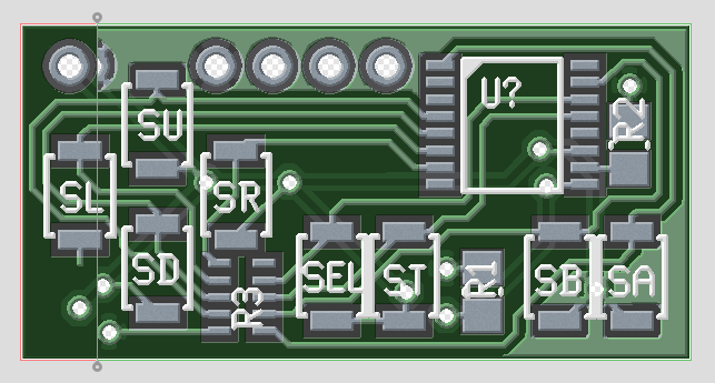
I was recently trying to add an image to a PCB I was making. Being so modular, gEDA pcb does not have an image import feature but instead relies on the program “pstoedit” to convert PostScript vector images into gEDA pcb objects. I have tried doing this before, but usually ended up with poor results. I finally collected the steps necessary to get repeatable, high quality results, which I will document here for anyone else trying to do the same.

1) Load your vector image into Inkscape (I will assume that you already have a vector image and have Inkscape installed)

2) Ensure your image uses only a single colour: black. All black objects will be added to your pcb object and all empty space will be left empty

3) Convert all objects to paths by selecting each object and using Path -> Object to path

4) Remove all overlapping vector paths by using Inkscape’s merging tools (union, difference, intersection, exclusion, division, etc) found in the Paths menu. If you end up with any paths that are touching (or are even just too close to each other without being joined) you are likely to end up with gEDA pcb carving gaps between them to meet the specified tolerances.

5) Adjust the file size to be appropriate for the scale it will be on the board. I have not yet found a way to reliably re-size the imported image once in pcb, so it is important to get this step right.

6) Save your image as a *.ps (PostScript) file. Make sure the “Convert texts to paths” box is marked. You may also want to have the “Resolution for rasterization (dpi)” setting cranked up to its maximum of 10000, but since the graphic remains a vector through this whole process, I don’t think it will make any difference (I haven’t tried playing with that number yet).

7) From the command line, change to the directory that your *.ps file is in and run a command like this:

$ pstoedit -psarg "-r1000x1000" -f pcbfill -ssp 'inputfile.ps' 'outputfile.pcb'

When I was first doing this, I didn’t add any of the optional parameters and I was using ‘pcb’ instead of ‘pcbfill’. -f pcbfill helps to ensure that the objects generated are solid, filled objects, which they might not be otherwise. -ssp forces things like letters with holes (‘o’, ‘d’, ‘p’, etc.) to convert correctly. The man page warns that this may be CPU intensive, but all the conversions I have done have run pretty well instantaneously. I also found I needed the -psarg “-r1000x1000” to get a good resolution out of the conversion.

8) Open your new *.pcb file in gEDA pcb and see the results. You may need to tweak some numbers or add/remove arguments, but so far this seems to work alright for me. Another option that might allow for a little more flexibility is including -xscale and -yscale flags if your image isn’t quite the right size. It may even help to make the image too large on purpose and the use the scaling flags to condense the resolution (again, I don’t think anything is rasterized during this process so I doubt this will make a difference, but it might be worth fiddling with it, even if I haven’t). You might also want to move the object into the top left corner of the pcb layout so that, in case you load it in a layout that is smaller it will still be visible.

9) At this point, you are ready to load your newly created pcb object into your full pcb project.

This process is not an exact science. Play with it until you find something you like. I have had success leaving out some of these steps too, so there is no need to redefine any defaults. Have any other tips for pcb graphics? Leave a comment!


2012
05.17

A while ago I read this excellent article by Evil Mad Scientist Laboratories describing the need for some form of visual diff tool for open hardware projects. I had been thinking this was a great idea, but while working on a recent project, decided to actually start implementing something. I use the gEDA suite of tools, so that is what I’m creating this for, but the majority of the plumbing should be reusable for other file formats.

The first piece of this puzzle for me was automatically making image files of my schematics and PCBs that have changed and adding them to each commit. GitHub has image diffing capabilities built in, so this works great. I implemented this a pre-commit hook in .git/hooks/. My git hooks can be found here. I have designed them to work with the git-hooks tool by Benjamin Meyer.

This script seems to work fine for me, though I’m open to suggestions for improvements. My major issues with how the hooks work (which are more issues with git than my hook) are

  1. The status message in the auto-generated commit comments is not being updated with the new image files and
  2. Hooks don’t get pushed into remotes

The first issue feels like a bug to me, but I suspect that it was done intentionally for some reason I’m not aware of. I have played with a work around by adding a prepare-commit-msg hook that just regenerates the commit message comments, but I have tested the pre-commit hook enough that I don’t feel I need to be aware of the addition of the images.

The second issue I am told is a security issue as it would cause arbitrary code to be executed on the machines of others who might clone (and possibly even the server). One nice feature of the git-hooks tool is that it can use hooks in a local repo directory, so if you include my scripts in the git_hooks repository, you just need to run ‘git hooks –install’ and you will have the hooks working. Without that tool, you can just manually copy them into the proper file in the .git/hooks/ directory.

This method works well if I want to view visual diffs online, but sometimes I might be offline or perhaps I just don’t want to push my project to a public GitHub repo. For that, I plan to make some simple scripts that call visual diffing tools on my local repository. Git has the capability to set your git diff tool, so my plan is to write a wrapper script that picks the right tool based on file types. This script might also generate an image from files that cannot be diffed directly and don’t have the above auto generated files

Edit: Of course not 20 minutes after I publish this post I discover schdiff, a tool bundled with gEDA since the start of 2012 that is designed to hook into git-difftool to provide a visual diff of gschem .sch files. One format down, some more to go.  :)

Edit 2: Less than a day later and I discover there is also a pcbdiff tool on my computer that came with gEDA pcb. In Arch Linux, it installs to /usr/share/pcb/tools/pcbdiff, but it is not in the path, so in my .bashrc I just added ‘export PATH=”$PATH:/usr/share/pcb/tools”‘ at the end. I feel pcbdiff outputs images that are too low a resolution, plus it can’t handle when the .pcb files change in physical size, so I might submit a patch or two. Long story short, now I just need to make a script that auto-calls these diff tools based on the file type.

2011
10.06

Photo "borrowed" from Leif Norman (click image for source)

This past Saturday was Nuit Blanche here in Winnipeg. Some 30,000 people went around the city checking out various exhibits of art and culture. One of the exhibits at the art gallery was ARTcadia. A bunch of displays setup with indie games and hacks. I had the NES-chuck out again and it saw a lot of use. Click here for some more pictures from the WAG.

While similar to Re:Play, the core difference for this event was that the games were setup as displays rather than booths. Because of this, there wasn’t someone around to provide instructions on how to start the game (ie. how to access the start and select buttons). We had a sign up with some instructions, but few people showed any interest in reading the signs. I may have to re-evaluate how this thing works for any future public displays.

CBC was running a contest called “Culture Vulture” where you have to go to cultural events and text in the posted word for an entry. SkullSpace must be getting some attention because the keyword posted at the WAG was “hacker”.

2011
08.17

NES-chuck Demo from Benjamin Bergman on Vimeo.

I finally got around to making a quick demonstration of my NES-chuck. Code for the NES-chuck can be found here. The future event I mention is ArtCadia, which is part of Nuit Blanche. I’m not yet sure if I (or the NES-chuck) can attend, but I will keep this updated.

After the break, there is a rough draft of my script for the video.

Read More >>