08.20
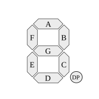
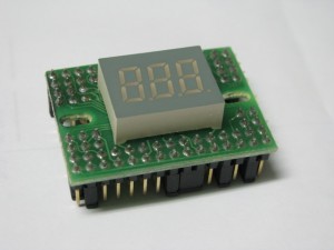
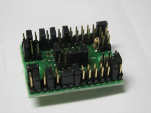
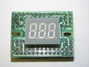
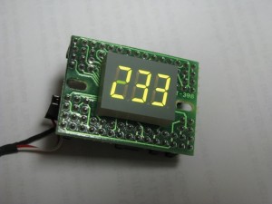 Well, I have got the board all powered up (I found “G” and “5V” silk screen markings hiding under one of the headers) and I think I have mostly figured out all the jumpers. There are two jumpers which I have called X and Y and the rest of the jumpers I have divided into sets R and S. The segments of the SSD I will refer to according to the following diagram from Wikipedia, with the leftmost digit being digit one and the right most digit being digit 3.
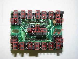
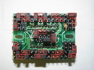
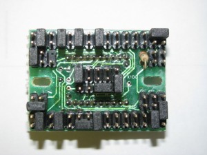
The jumper sets R and S are as follows:
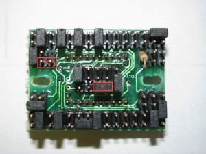
Jumpers X and Y are found here:
Using Karnaugh maps, which I always find fun, the X and Y jumpers can be used to enable/disable header sets R and S.
__|X|~X|                 __|X|~X|
Y |0| 1|                 Y |0| 1|
~Y|1| 1|                 ~Y|0| 0|
Map for header set R     Map for header set S
This simplifies to R = ~X + ~Y and S = ~XY (ie. set R is enabled when either jumper X is removed OR jumper Y is removed and set S is enabled when when jumper X is removed AND jumper Y in installed). At first I thought that this setup might be so they could plop a bunch of headers in and be able to just swap around the X and Y configuration to get different readouts, but I don’t really see that being feasible with how this is all setup.
There are also a bunch of headers that don’t seem to do anything (every fourth set in the top and bottom rows). Perhaps it was just cheaper to install a wide set of headers than to install a few broken sections. Having set R spaced at every other header makes it easy to place jumpers so a dead space does make sense. There are traces I can see to some of these pins, but I suspect they are just grounded so that they don’t light anything. There is also a pin missing just above the X header. On the back side of the PCB you can see there is a via almost in the spot where the header pin should have been, but not quite exactly. If they really put the big headers in to save money/time, why pull this pin out of the header block? The via would have worked just as well if there was a pin soldered in the hole. The via connects from common B1 pin to the SSD, so that pin was likely removed to prevent the B1 segment from being lit by a jumper near X.
