08.20
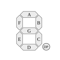
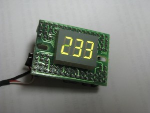 Well, I have got the board all powered up (I found “G” and “5V” silk screen markings hiding under one of the headers) and I think I have mostly figured out all the jumpers. There are two jumpers which I have called X and Y and the rest of the jumpers I have divided into sets R and S. The segments of the SSD I will refer to according to the following diagram from Wikipedia, with the leftmost digit being digit one and the right most digit being digit 3.
The jumper sets R and S are as follows:
Jumpers X and Y are found here:
Using Karnaugh maps, which I always find fun, the X and Y jumpers can be used to enable/disable header sets R and S.
__|X|~X|                 __|X|~X|
Y |0| 1|                 Y |0| 1|
~Y|1| 1|                 ~Y|0| 0|
Map for header set R     Map for header set S
This simplifies to R = ~X + ~Y and S = ~XY (ie. set R is enabled when either jumper X is removed OR jumper Y is removed and set S is enabled when when jumper X is removed AND jumper Y in installed). At first I thought that this setup might be so they could plop a bunch of headers in and be able to just swap around the X and Y configuration to get different readouts, but I don’t really see that being feasible with how this is all setup.
There are also a bunch of headers that don’t seem to do anything (every fourth set in the top and bottom rows). Perhaps it was just cheaper to install a wide set of headers than to install a few broken sections. Having set R spaced at every other header makes it easy to place jumpers so a dead space does make sense. There are traces I can see to some of these pins, but I suspect they are just grounded so that they don’t light anything. There is also a pin missing just above the X header. On the back side of the PCB you can see there is a via almost in the spot where the header pin should have been, but not quite exactly. If they really put the big headers in to save money/time, why pull this pin out of the header block? The via would have worked just as well if there was a pin soldered in the hole. The via connects from common B1 pin to the SSD, so that pin was likely removed to prevent the B1 segment from being lit by a jumper near X.
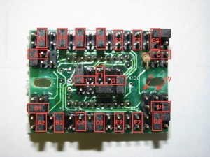
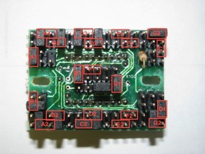
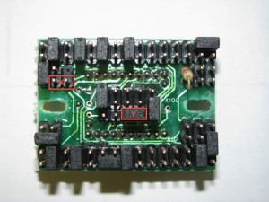
Any thoughts on what that ‘x10’ and ‘x100’ refer to?
I think the x100 and x10 are indicators for which header cluster is for which digit. A1, B1, C1, etc. is for the digit in the 100’s place and A2, B2, etc. is for the digit in the 10’s place. Many of the 100’s headers are on that centre cluster and all of the 10’s headers are in the lower section. Since the x10 and x100 aren’t really next to anything more obvious (such as specific pins or unused solder pads), that will have to be my answer.
I was also thinking a little more on the purpose of the X and Y headers. Perhaps jumper Y is really only to cross a power lead over traces on the PCB. Maybe that is the one spot where the number of layers in the thing was insufficient. Why header X is there is still a mystery. it is next to the gap where a pin should be, so it would seem that it is intended for a jumper to be placed where I placed one.