Category: Free Software
2012
05.27

When working on my personal projects, I tend to use as much open source software as possible. Many people in the hobbyist world use Eagle for their EDA tools, which has a free restricted version but is not open. I personally prefer to use the gEDA suite of tools. I like it for its cross platform compatibility and its adherence to the Unix philosophy of “do one job and do it well” allowing tools to be connected in many different ways. This often allows the tools to be leaner, yet more powerful. This can also often make some of these tools a bit harder to pick up.

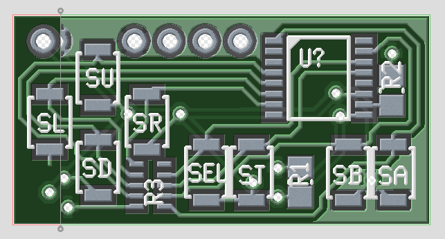
I was recently trying to add an image to a PCB I was making. Being so modular, gEDA pcb does not have an image import feature but instead relies on the program “pstoedit” to convert PostScript vector images into gEDA pcb objects. I have tried doing this before, but usually ended up with poor results. I finally collected the steps necessary to get repeatable, high quality results, which I will document here for anyone else trying to do the same.

1) Load your vector image into Inkscape (I will assume that you already have a vector image and have Inkscape installed)

2) Ensure your image uses only a single colour: black. All black objects will be added to your pcb object and all empty space will be left empty

3) Convert all objects to paths by selecting each object and using Path -> Object to path

4) Remove all overlapping vector paths by using Inkscape’s merging tools (union, difference, intersection, exclusion, division, etc) found in the Paths menu. If you end up with any paths that are touching (or are even just too close to each other without being joined) you are likely to end up with gEDA pcb carving gaps between them to meet the specified tolerances.

5) Adjust the file size to be appropriate for the scale it will be on the board. I have not yet found a way to reliably re-size the imported image once in pcb, so it is important to get this step right.

6) Save your image as a *.ps (PostScript) file. Make sure the “Convert texts to paths” box is marked. You may also want to have the “Resolution for rasterization (dpi)” setting cranked up to its maximum of 10000, but since the graphic remains a vector through this whole process, I don’t think it will make any difference (I haven’t tried playing with that number yet).

7) From the command line, change to the directory that your *.ps file is in and run a command like this:

$ pstoedit -psarg "-r1000x1000" -f pcbfill -ssp 'inputfile.ps' 'outputfile.pcb'

When I was first doing this, I didn’t add any of the optional parameters and I was using ‘pcb’ instead of ‘pcbfill’. -f pcbfill helps to ensure that the objects generated are solid, filled objects, which they might not be otherwise. -ssp forces things like letters with holes (‘o’, ‘d’, ‘p’, etc.) to convert correctly. The man page warns that this may be CPU intensive, but all the conversions I have done have run pretty well instantaneously. I also found I needed the -psarg “-r1000x1000” to get a good resolution out of the conversion.

8) Open your new *.pcb file in gEDA pcb and see the results. You may need to tweak some numbers or add/remove arguments, but so far this seems to work alright for me. Another option that might allow for a little more flexibility is including -xscale and -yscale flags if your image isn’t quite the right size. It may even help to make the image too large on purpose and the use the scaling flags to condense the resolution (again, I don’t think anything is rasterized during this process so I doubt this will make a difference, but it might be worth fiddling with it, even if I haven’t). You might also want to move the object into the top left corner of the pcb layout so that, in case you load it in a layout that is smaller it will still be visible.

9) At this point, you are ready to load your newly created pcb object into your full pcb project.

This process is not an exact science. Play with it until you find something you like. I have had success leaving out some of these steps too, so there is no need to redefine any defaults. Have any other tips for pcb graphics? Leave a comment!
 

2012
05.27

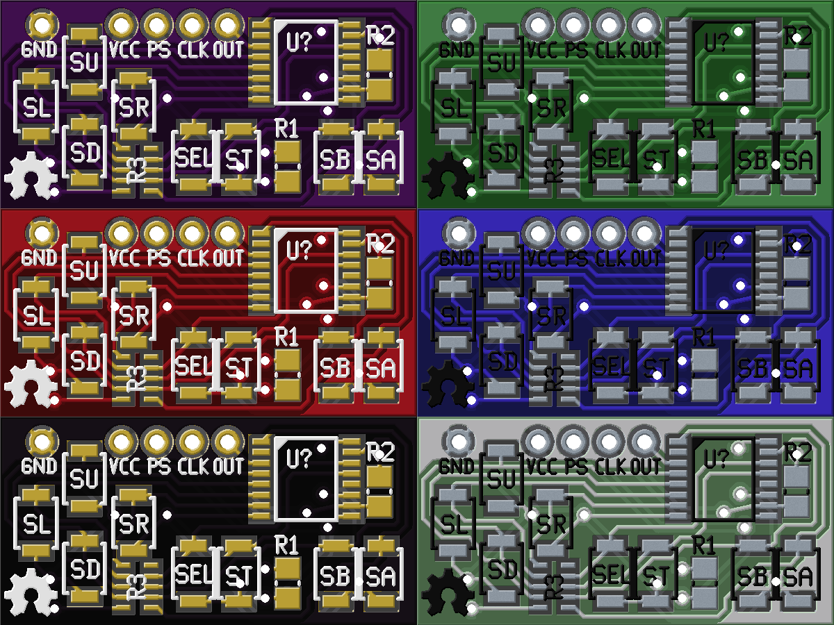
While working on a project this week, I was trying to see what some silk screen art would look like on a PCB I’m working on, but the “photo realistic” export mode of gEDA pcb was restricted to only green solder mask, tin plating, and white silk screen. The fab house I plan to use only provides purple solder mask, gold plating, and white silk screen. Rather than try to tweak the green image in GIMP until it looks half decent, then repeating the process for each candidate silk screen image (and then each future project as well), I decided I would just write a patch!

My patch for gEDA pcb allows the user to now select a solder mask colour of green, blue, red, purple, black, or a (questionable) white, a pad plating colour of regular tin or gold, and a silk screen colour of white or black. All of these options are pictured above. You can find my proposed patch here, and hopefully it be accepted into the core software soon so that you can get it from your system’s repository.

I’ve been a fan and advocate of open source software for some time now, but I am pretty sure that this is the first time that I have actually submitted a patch to a somewhat mainstream open source project. I’m pretty pumped and I hope to do more soon. I heartily recommend it.

Update 2012-06-14: After some suggested improvement to my patch (additional yellow silk as well as the addition of copper and silver pad plating) my patch has officially been accepted into the gEDA pcb repository! You can get the latest version of the code here: git clone git://git.geda-project.org/pcb.git

2012
05.17

A while ago I read this excellent article by Evil Mad Scientist Laboratories describing the need for some form of visual diff tool for open hardware projects. I had been thinking this was a great idea, but while working on a recent project, decided to actually start implementing something. I use the gEDA suite of tools, so that is what I’m creating this for, but the majority of the plumbing should be reusable for other file formats.

The first piece of this puzzle for me was automatically making image files of my schematics and PCBs that have changed and adding them to each commit. GitHub has image diffing capabilities built in, so this works great. I implemented this a pre-commit hook in .git/hooks/. My git hooks can be found here. I have designed them to work with the git-hooks tool by Benjamin Meyer.

This script seems to work fine for me, though I’m open to suggestions for improvements. My major issues with how the hooks work (which are more issues with git than my hook) are

  1. The status message in the auto-generated commit comments is not being updated with the new image files and
  2. Hooks don’t get pushed into remotes

The first issue feels like a bug to me, but I suspect that it was done intentionally for some reason I’m not aware of. I have played with a work around by adding a prepare-commit-msg hook that just regenerates the commit message comments, but I have tested the pre-commit hook enough that I don’t feel I need to be aware of the addition of the images.

The second issue I am told is a security issue as it would cause arbitrary code to be executed on the machines of others who might clone (and possibly even the server). One nice feature of the git-hooks tool is that it can use hooks in a local repo directory, so if you include my scripts in the git_hooks repository, you just need to run ‘git hooks –install’ and you will have the hooks working. Without that tool, you can just manually copy them into the proper file in the .git/hooks/ directory.

This method works well if I want to view visual diffs online, but sometimes I might be offline or perhaps I just don’t want to push my project to a public GitHub repo. For that, I plan to make some simple scripts that call visual diffing tools on my local repository. Git has the capability to set your git diff tool, so my plan is to write a wrapper script that picks the right tool based on file types. This script might also generate an image from files that cannot be diffed directly and don’t have the above auto generated files

Edit: Of course not 20 minutes after I publish this post I discover schdiff, a tool bundled with gEDA since the start of 2012 that is designed to hook into git-difftool to provide a visual diff of gschem .sch files. One format down, some more to go.  :)

Edit 2: Less than a day later and I discover there is also a pcbdiff tool on my computer that came with gEDA pcb. In Arch Linux, it installs to /usr/share/pcb/tools/pcbdiff, but it is not in the path, so in my .bashrc I just added ‘export PATH=”$PATH:/usr/share/pcb/tools”‘ at the end. I feel pcbdiff outputs images that are too low a resolution, plus it can’t handle when the .pcb files change in physical size, so I might submit a patch or two. Long story short, now I just need to make a script that auto-calls these diff tools based on the file type.

2011
04.02

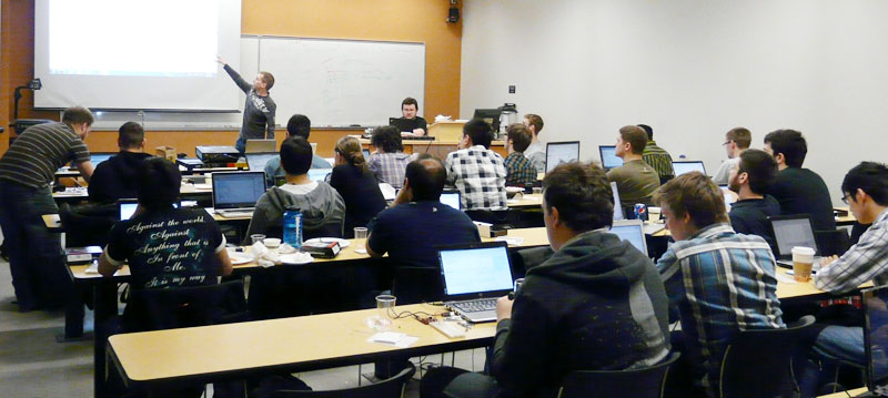
Last Sunday, UMIEEE together with UMARS (two University of Manitoba student groups I am a part of) got together to hold an embedded systems workshop on campus. We helped teach a bunch of fellow students the basics of designing and programming embedded systems. We used TI’s MSP430 Launchpad development kit, a super low price dev kit, so that everyone could go home with their project and continue experimenting. While the Launchpad (or rather the MSP430 microcontroller on the board) isn’t as easy to program as something like an Arduino, the Launchpad allowed us to convey some of the more fundamental principles of embedded design like bit masking and timer interrupts.

The morning consisted of getting the tools setup and getting a “hello world” application running. The official tools are Windows only, but the Launchpad does work with Mac and Linux once you figure out how to install everything. It actually seemed to work better, due partly to the fact that the tools are open source and hence not crippled versions of paid software, but also because the environment was less integrated (ie you use a text editor, a compiler, and a debugger all separately instead of a full blown IDE like they use in Windows). The Windows users ofter had to restart the whole IDE when one part of the system locked up for unknown reasons.

After lunch, we dove into making a much more ambitious project: an LED chaser. The design specifications we gave to everyone was something to the effect of “when you press a button, your chain of LEDs will light up one by one until you reach the final one in the string.” The idea was then to replace the final LED with the next person’s button input pin and watch as the lit LED ran across everyone’s boards. The day before, the volunteers leading the workshop got together and pumped out a quick (and admittedly buggy) code for this, so we felt it was an attainable project. We nudged everyone along, showing them how to light individual LEDs, use interrupt pins and timers, and wire up buttons with pull up resistors. I think only a few people actually got the final chaser working, but everyone had a good time.

You can see an abstract for the event along with a bunch more pictures here.

2011
02.24

At the end of last year, Microsoft launched the Kinect, a motion tracking add-on for the Xbox 360 gaming platform. Adafruit Industries, an open source hobbyist hardware company, announced that they would be offering a bounty to whomever first released an open source driver for the Kinect. The bounty started at $1000, but each time Microsoft complained about it, they raised the bounty. After only a week, the bounty had increased to $3000 and was awarded to a man in Spain. Within a few weeks of that, and having seen all of the interesting things that people were doing with the Kinect (and the large volume of sales they were receiving because of it), Microsoft changed their story, saying that they had originally left the Kinect open for such 3rd party projects.

I followed the story pretty much from the beginning and it was pretty interesting to see how things progressed. However, a few days ago Johnny Lee, a former developer of the Kinect and author of the Procrastineering blog, announced that he had been pushing for Microsoft to release Kinect drivers, but that they were unwilling. As a result, he had sponsored Adafruit to organize the Open Kinect challenge. While it probably would have been in Microsoft’s best interests to release the driver themselves, keeping Kinect development largely done on their platform, the Open Kinect challenge made a cross platform driver available which ends up benefiting everyone.